iBeam Materials (SWITCHES)
LOW-COST LEDS ON FLEXIBLE METAL TAPES
UPDATED: JANUARY 27, 2017
PROJECT TITLE: Epitaxial GaN on Flexible Metal Tapes for Low-Cost Transistor Devices
PROGRAM: Strategies for Wide Bandgap, Inexpensive Transistors for Controlling High-Efficiency Systems (SWITCHES)
AWARD: $2,768,468
PROJECT TEAM: iBeam Materials (Lead), Sandia National Laboratory, Los Alamos National Laboratory, University of New Mexico
PROJECT TERM: March 2014 – October 2017
PRINCIPAL INVESTIGATOR (PI): Dr. Vladimir Matias
TECHNICAL CHALLENGE
Lighting constitutes approximately 10% of the total U.S. electricity consumption. The U.S. Energy Information Administration (EIA) estimates that in 2015, about 404 billion kilowatt hours (kWh) of electricity were used for lighting in the United States, but most of that energy is wasted as heat. Solid-state lighting (SSL), such as a light-emitting diode (LED) bulb, uses a semiconductor as its light source. Consumer’s savings for using SSL are large because SSL uses only a fraction of the electricity of traditional lighting methods and can last far longer. The U.S. Department of Energy estimates that rapid adoption of LED lighting over the next 20 years in the United States could cumulatively save about $630 billion in energy costs by reducing electricity use by 18.5 trillion kilowatt hours, equivalent to the output of 100 new power plants. However, despite recent technological advances and rapid decreases in cost, the initial cost of units is still a barrier to wide acceptance.
TECHNICAL OPPORTUNITY
Currently LEDs used for general lighting are manufactured from gallium nitride (GaN) layers deposited on small, expensive, single-crystal wafer substrates such as sapphire or silicon carbide. This type of manufacturing limits the production of LEDs to discrete chips that need to be diced from the substrate, packaged into a surface mounted device (SMD), and placed in a luminaire (bulb) using costly pick-and-place (P&P) technology. Because many LED applications do not require consistent high quality substrates over large areas, they are potentially amenable to a new manufacturing process using inexpensive substrates in a continuous roll-to-roll (R2R) method. This would also allow elimination of SMDs and P&P, as the LED strips and sheets could be used directly as lighting devices. Replacing the expensive small scale substrate along with considerably simplifying the LED luminaire will help to reduce costs and stimulate wider adoption of LED lighting.
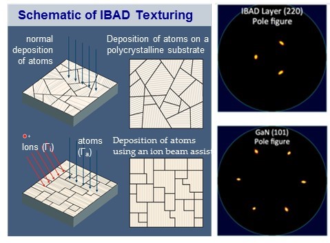
Figure 1: Schematic of IBAD texturing. Bombardment by ions creates preferred orientations for growth, reducing crystalline mismatch across the substrate.
INNOVATION DEMONSTRATION
The iBeam Materials team’s goal is to develop a scalable manufacturing method to produce low-cost (10x reduction) GaN LED devices on flexible metal foils for use in solid-state lighting. The fabrication process uses an ion-beam crystal-aligning process (ion beam assisted deposition, IBAD[1]) to create preferred growth orientations on arbitrary substrates, such as thin, flexible metal foils, which eliminate the need for expensive single-crystal substrates.
The technical goals of this project are to demonstrate a large area LED light strip prototype on a 40 x 5 mm flexible metal foil with a luminance of >50,000 candela per square meter (cd/m2) or, assuming 3 steridians, 30 lumens, comparable to a typical flashlight. The iBeam team first identified an appropriate metal substrate, molybdenum that can be obtained in thin sheets or rolls and has a coefficient of thermal expansion matching GaN, which makes it ideal for the IBAD process. They then developed a process called solution deposition planarization (SDPTM) to planarize the starting metal substrate over large areas by repeatedly depositing smoothing layers. The SDP layer provides the smoothness needed for the IBAD process and also provides the appropriate base layer for IBAD texturing and a barrier to interdiffusion from the substrate.
After planarization, a buffer layer, typically an oxide layer, is deposited on the metal foil and aligned using an ion beam assisted deposition as illustrated in Fig. 1. An initial challenge faced by iBeam was that typical IBAD buffer layer materials have (100) oriented cubic crystal structure with a 4-fold symmetry, which is not compatible with the hexagonal crystal structure of gallium nitride. To overcome this challenge, iBeam developed a (111) orientated buffer layer with 3-fold symmetry to accommodate the hexagonal crystal structure of gallium nitride.
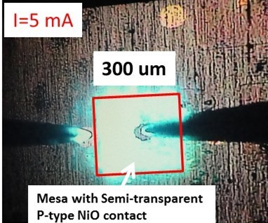
Figure 2: First-in-the-world GaN LED device fabricated directly on a metal foil.
iBeam Materials worked with Sandia National Laboratories to develop a metal-organic chemical vapor deposition (MOCVD) process for depositing epitaxial GaN and other LED device layers on their IBAD templates. They demonstrated gallium nitride growth with dislocation densities of ~ 8x108 cm-2, comparable to that achieved on single-crystal wafer templates such as sapphire. They then fabricated GaN LED devices directly on their metal-foil supported GaN layers, and demonstrated light emission with no degradation after bending strips to a radius of 7mm. The LEDs fabricated on iBeam’s IBAD template exhibited an internal quantum efficiency (IQE)[2], greater than 70% of the devices fabricated in the same manner on sapphire. The external quantum efficiency (EQE), which defines how efficiently the device converts electrons into photons that actually escape from the device and contribute to luminosity, was 13-17% of similar LEDs fabricated on sapphire without any light extraction optimization. Further work is underway to improve the IQE and EQE of LEDs fabricated on iBeam’s IBAD metal substrates. The team is also continuing to improve their IBAD process to reduce cost and improve the performance of LEDs fabricated on the single-crystal-like templates.
The SDPTM and the IBAD processes developed by iBeam are implemented in a continuous R2R deposition, while the GaN MOCVD at Sandia is done in a wafer batch process. Implementing R2R MOCVD for GaN should bring down epiwafer costs by a factor of two, but more cost-effective GaN processes would bring costs down even further. Further significant cost savings are expected from the simplification of the LED packaging since the LEDs come pre-packaged on the metal sheet with the metal substrate acting both as a reflector and heat sink. Contacts and phosphors can be applied using a printing technology.
PATHWAY TO ECONOMIC IMPACT
The iBeam team has identified a path to market based on the flexible nature of this inorganic LED technology. One of the first-market applications under consideration is horticulture lighting. The iBeam light strip form factor will distribute light with a lower power density and lower heat density than traditional light sources, making it cool enough for leaf contact and enabling an ‘intra-canopy’ lighting breakthrough product. Ultimately, iBeam sees developing light emitting strips that will enable a cost-competitive LED replacement for the fluorescent light tubes that dominate commercial lighting markets. iBeam’s goal is for their light strip to cost less than $0.1/klm (figure based on iBeam’s projections), more than half the cost of conventional LED lighting systems.
The U.S. Department of Energy (DOE), Office of Energy Efficiency & Renewable Energy (EERE) has awarded iBeam funding under the new Small Business Vouchers (SBV) Pilot Program totaling $225,000. iBeam has also been awarded funding through the New Mexico Small Business Assistance (NMSBA) in the amount of $20,000 per year for the last three years for work performed at the National Labs.
The team is developing connections with venture capital investors as a potential pathway to further commercial development. Other applications in display and wearable markets are also being explored.
LONG-TERM IMPACTS
SSL offers a great opportunity to reduce electricity consumption, thereby improving domestic energy security and reducing greenhouse emissions. iBeam’s goal is for their IBAD technology to lower the cost of LED substrates to as low as $50/m2 (current market rate of sapphire substrates is about $20,000/m2) and reduce the cost for luminaire manufacturing using a scalable R2R process eliminating several manufacturing steps. The reduced cost could enable widespread deployment of efficient LED-based solid-state lighting (SSL), and potentially generate sales opportunities outside the United States.
INTELLECTUAL PROPERTY AND PUBLICATIONS
The iBeam team’s project has generated one U.S. Patent and Trademark Office (PTO) patent application.
[1] Vladimir Matias and Robert H. Hammond, Surf. Coat. & Tech. 264, 1 (2015).
[2] the proportion of all recombinations in the active region that produce light