Massachusetts Institute of Technology (ADEPT)
POWERCHIP TO POWER THE WORLD
UPDATED: JUNE 22, 2016
PROJECT TITLE: PowerChip: Advanced Technologies for Integrated Power Electronics
PROGRAM: Agile Delivery of Electric Power Technology (ADEPT)
AWARD: $4,414,003
PROJECT TEAM: MIT (Lead), Dartmouth College, University of Pennsylvania, Georgia Tech
PROJECT TERM: September 1, 2010 – December 31, 2013
PRINCIPAL INVESTIGATOR (PI): Prof. David Perreault
TECHNICAL CHALLENGE
Conversion of electrical power from one form to another is achieved by power electronics. The application area is very broad as power electronics is the bottleneck in key systems such as solid-state lighting, solar and wind converters, motor drives (escalators, elevators, home appliances, HVAC), hybrid and electrical vehicles, and energy needs of rapidly growing data centers. Energy losses in the conversion processes themselves are significant, and even larger opportunities for energy savings exist in improved performance of the devices that are driven by the converted power. Low loss, low-cost power conversion that can switch rapidly and maintain high-quality waveforms is needed to enable gains in energy efficiency across the application areas.
TECHNICAL OPPORTUNITY
The development of new wide bandgap semiconductor materials has opened new opportunities for higher energy efficiency and performance reliably in power electronics. Wide bandgap semiconductor devices can operate at far higher frequencies and with significantly lower losses than incumbent Si-based transistors and thyristors. However, the wide bandgap semiconductors devices are only part of a complete power converter, which also requires inductors and transformers. These are based on magnetic materials, where advances in nano-structured materials offer the potential for improved properties. Novel circuit architectures, topologies, and designs are required to exploit the progress made in semiconductor devices and magnetic components to achieve higher performance and greater system miniaturization. Successful development in this area draws on advances in semiconductor devices, magnetic components, and circuit aspects of the power system simultaneously.
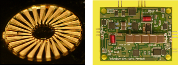
Figure 1: Microfabricated coreless inductor (left) and high frequency DC-to-DC converter (right)
INNOVATION DEMONSTRATION
Under ARPA-E support, the MIT project addressed all three areas needed to improve power conversion: switching devices, inductors, and circuit design. The goals of the project team were: to exploit the potential of GaN for high-power switching in practical, reliable devices; to create high-frequency inductors by developing new materials and designs; and to create overall circuit designs for power converters that optimally integrated the new components. As a final deliverable, the team aimed to integrate the innovations into a 10 – 50 W power converter with an input of 100 V, > 93% efficiency, 5 MHz switching frequency, and power density of 300 W/in3.
First, enhancement-mode gallium nitride (GaN) high electron mobility transistors (HEMTs) capable of withstanding 600 V were made. This advance is notable because GaN devices are typically depletion mode (normally-on), requiring more complex circuit design and affecting system reliability. MIT developed a new (tri-gate) design, reduced defect states with new etching and passivation approaches, controlling defects during GaN growth, and engineering the electric fields in the device to increase breakdown voltage. At the time of the project, there were a few commercial examples of GaN devices rated for 600 V, but those were based on depletion-mode devices. The MIT team was able to push the state-of-the-art 600 V operation in enhancement-mode.
Second, the team increased the power density of the converters by creating inductive elements capable of switching at 5 MHz, thereby shrinking their size. Georgia Tech used microelectromechanical (MEMS) fabrication processes to create solenoid and toroid inductors with and without magnetic cores, while drastically reducing the fabrication time and cost. Inductance values ranged from 60 – 800 nH and small signal quality factors were 8-45, which are comparable to commercial devices with a larger footprint.[1] In parallel, the team developed magnetic core materials to achieve a higher efficiency and inductance with fewer inductor turns. These materials were then integrated with microfabricated toroids or hand-wound inductors made by Georgia Tech. Dartmouth created new core magnetic core materials from sputter-deposited Co-Zr-O nanocomposites; by applying a magnetic field during deposition, the team produced a material with local anistropy that allowed them to achieve an efficiency of 96% and quality factor of 50 over the 10 – 50 MHz range. UPenn developed nanocomposite magnetic core materials with high permeability but low dielectric loss. They key was creating nanoscaled particles with nearly identical sizes. When integrated into toroidal micro-inductors, they demonstrated an efficiency of 93% at 5 MHz and a 40 W load.
Another group at MIT analyzed and optimized the design of the full range of microfabricated cored and coreless inductors. They developed models to estimate the energy stored and power dissipated and built an equivalent circuit model to analyze the performance over a wide range of inductor designs and transistor sizes. The results were used to design the inductors used in the final LED driver deliverable for the project.
Finally, MIT developed new circuit topologies to take advantage of the enhancement-mode GaN HEMTs and the high-frequency inductors. A two-stage architecture was created to accommodate frequencies of 3 – 30 MHz and a wide range of DC or AC input. The team demonstrated a DC-to-DC LED driver with an input of 100 V and output power of 41 W. The efficiency was 94% and the box power density was 406 W/in3. The team also built an AC-to-DC converter with an efficiency of 93.3% and power factor of 0.89 at frequencies between 3 – 30 MHz, achieving an overall box power density of 50 W/in3. Current LED drivers operate in a frequency range of 50 – 100 kHz, have a maximum efficiency of 85%, and power density < 5 W/in3.
PATHWAY TO ECONOMIC IMPACT
The project showed a proof of principle that a broad range of input voltages could be accommodated by one converter at high frequencies. The test circuits at MIT demonstrated higher efficiencies and power densities than larger, commercial circuits. In June 2016, an MIT spinout company named FINsix began shipping DART, a 65 W laptop charger that is three times smaller and lighter than conventional chargers. The circuit design concepts created during the ARPA-E project and the lessons learned directly informed the design of the DART charger. In January 2016, FINsix and Lenovo announced a partnership to make the smaller charger available for select ThinkPad models. Concurrently, the team is collaborating with major power electronics companies such as Texas Instruments to design converters in the range of tens to hundreds of Watts. LED drivers are a second initial market.
The novel GaN transistor technology developed during the project was the key IP to start the company Cambridge Electronics (http://www.gantechnology.com). This company, started by students whose research was originally funded by the ARPA-E project, licensed the IP from MIT and is currently offering state-of-the-art GaN devices for sale to selected partners. The company has received numerous awards, including the Massachusetts’ MassVentures Start Award (Phase I and II) as well as the 2016 Compound Semiconductor Industry Award (http://www.csawards.net/).
LONG-TERM IMPACTS
The MIT project has proven the viability of shrinking power converters by moving to higher frequencies. Smaller form factors will accelerate deployment of LEDs and reduce the size of converters for widespread technologies such as laptops. The team also demonstrated efficiencies greater than 90%, compared to 85% today. If every new laptop shipped in the United States had this higher efficiency, it would save 46 gigawatt-hours of electricity per year. Furthermore, the team’s research in the field of magnetic materials for inductors could revolutionize how power converters are designed and operated. Existing commercial materials with low magnetic permeability could be incorporated into these new circuit designs at frequencies such as 10 MHz, drastically increasing the power density from 5 W/in3 to more than 300 W/in3 while reducing electrical losses.
INTELLECTUAL PROPERTY AND PUBLICATIONS
As of June 2016, the MIT team’s project has generated nine invention disclosures to ARPA-E, seven non-provisional U.S. Patent and Trademark Office (PTO) patent applications, and two U.S. patents issued by PTO.
“Diode having trenches in a semiconductor region,” (3/22/2016) Patent No 9,293,538, Washington, DC: U.S. Patent and Trademark Office.
“Semiconductor devices having a recessed electrode structure,” (5/26/2015) Patent No 9,041,003, Washington, DC: U.S. Patent and Trademark Office.
The MIT team has also published the scientific underpinnings of this technology extensively in the open literature.
A list of publications is provided below:
Araghchini, M., Chen, J., Doan-Nguyen, V., Harburg, D. V., Jin, D., Kim, J., . . . Sullivan, C. R. (2013). A Technology Overview of the PowerChip Development Program. IEEE Transactions on Power Electronics IEEE Trans. Power Electron., 28(9), 4182-4201. doi:10.1109/tpel.2013.2237791
Araghchini, M., Yu, X., Kim, M. S., Qiu, J., Herrault, F., Sullivan, C. R., . . . Lang, J. H. (2014). Modeling and Measured Verification of Stored Energy and Loss in MEMS Toroidal Inductors. IEEE Transactions on Industry Applications IEEE Trans. on Ind. Applicat., 50(3), 2029-2038. doi:10.1109/tia.2013.2291991
Dong, A., Chen, J., Ye, X., Kikkawa, J. M., & Murray, C. B. (2011). Enhanced Thermal Stability and Magnetic Properties in NaCl-Type FePt–MnO Binary Nanocrystal Superlattices. J. Am. Chem. Soc. Journal of the American Chemical Society, 133(34), 13296-13299. doi:10.1021/ja2057314
Fafarman, A. T., Koh, W., Diroll, B. T., Kim, D. K., Ko, D., Oh, S. J., . . . Kagan, C. R. (2011). Thiocyanate-Capped Nanocrystal Colloids: Vibrational Reporter of Surface Chemistry and Solution-Based Route to Enhanced Coupling in Nanocrystal Solids. J. Am. Chem. Soc. Journal of the American Chemical Society, 133(39), 15753-15761. doi:10.1021/ja206303g
Jin, D., & Alamo, J. A. (2012). Impact of high-power stress on dynamic ON-resistance of high-voltage GaN HEMTs. Microelectronics Reliability, 52(12), 2875-2879. doi:10.1016/j.microrel.2012.08.023
Jin, D., & Alamo, J. A. (2013). Methodology for the Study of Dynamic ON-Resistance in High-Voltage GaN Field-Effect Transistors. IEEE Trans. Electron Devices IEEE Transactions on Electron Devices, 60(10), 3190-3196. doi:10.1109/ted.2013.2274477
Kim, J., Herrault, F., Yu, X., Kim, M., Shafer, R. H., & Allen, M. G. (2013). Microfabrication of air core power inductors with metal-encapsulated polymer vias. J. Micromech. Microeng. Journal of Micromechanics and Microengineering, 23(3), 035006. doi:10.1088/0960-1317/23/3/035006
Lu, B., Matioli, E., & Palacios, T. (2012). Tri-Gate Normally-Off GaN Power MISFET. IEEE Electron Device Lett. IEEE Electron Device Letters, 33(3), 360-362. doi:10.1109/led.2011.2179971
Lu, B., Sun, M., & Palacios, T. (2013). An Etch-Stop Barrier Structure for GaN High-Electron-Mobility Transistors. IEEE Electron Device Lett. IEEE Electron Device Letters, 34(3), 369-371. doi:10.1109/led.2012.2237374
Paik, T., Ko, D., Gordon, T. R., Doan-Nguyen, V., & Murray, C. B. (2011). Studies of Liquid Crystalline Self-Assembly of GdF 3 Nanoplates by In-Plane, Out-of-Plane SAXS. ACS Nano, 5(10), 8322-8330. doi:10.1021/nn203049t
Qiu, J., & Sullivan, C. R. (2013). High-Frequency Resistivity Measurement Method for Multilayer Soft Magnetic Films. IEEE Transactions on Power Electronics IEEE Trans. Power Electron., 28(7), 3581-3590. doi:10.1109/tpel.2012.2226477
Sullivan, C. R., Harburg, D. V., Qiu, J., Levey, C. G., & Yao, D. (2013). Integrating Magnetics for On-Chip Power: A Perspective. IEEE Transactions on Power Electronics IEEE Trans. Power Electron., 28(9), 4342-4353. doi:10.1109/tpel.2013.2240465
Yu, X., Kim, M., Herrault, F., Ji, C., Kim, J., & Allen, M. G. (2013). Silicon-Embedding Approaches to 3-D Toroidal Inductor Fabrication. Journal of Microelectromechanical Systems J. Microelectromech. Syst., 22(3), 580-588. doi:10.1109/jmems.2012.2233718
[1] See for instance: http://www.murata.com/en-us/products/inductor/chip/feature/rf, http://electronics.stackexchange.com/questions/190953/q-factor-in-inductors