1366 Technologies (OPEN 2009)
DIRECT MANUFACTURING OF SILICON WAFERS REDUCES COST AND IMPROVES PERFORMANCE
UPDATED: JUNE 28, 2016
PROJECT TITLE: Direct Wafer: Enabling Terawatt Photovoltaics
PROGRAM: OPEN 2009
AWARD: $4,000,000
PROJECT TEAM: 1366 Technologies
PROJECT TERM: March 2010 – June 2012
TECHNICAL CHALLENGE
Crystalline silicon wafers contribute 40% to the total cost of a solar cell module, making the wafer the largest single cost contributor to photovoltaic installed costs ($4/W in 2009). While much effort is focused towards increasing the efficiency of solar cells using new materials (i.e. CIGS, CdTe, and organic photovoltaics), little attention has been paid to reducing the cost of the silicon wafer itself. As silicon remains the only stable, earth-abundant material demonstrated to be capable of obtaining low cost, high efficiency, and commercial viability, cost reduction of the silicon wafer is crucial to further improve near-term commercial competitiveness of solar energy.
TECHNICAL OPPORTUNITY
Eliminating the most expensive and wasteful processes in silicon wafer manufacturing, casting and sawing, provides a strong potential to dramatically reduce the cost of manufacturing and increase silicon utilization. Traditional manufacturing requires sawing wafers from grown silicon ingots, which wastes approximately 50% of input silicon. Significant post-processing is also required to reduce impurities induced by sawing and achieve required wafer strength. Adoption of new, transformational manufacturing methods would impact the full silicon supply chain by reducing costs and enhancing production rates of silicon wafers, utimately enabling high penetration of low-cost solar cells, manufactured in the United States.
Figure 1: Solar module efficiencies continued improvement during the ARPA-E project period. The graphical representation (left) summarizes improvements and technical details are provided in the table (right).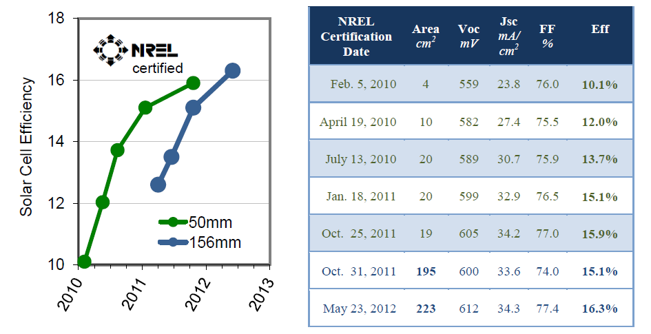
INNOVATION DEMONSTRATION
The molten silicon Direct WaferTM process developed by 1366 Technologies inherently reduces the cost and improves the strength and performance of the silicon wafer. The 1366 process of attaching molten silicon to a reusable substrate, solidifying a thin sheet, and cleanly releasing a wafer eliminates the need for the sawing process, allows for controllable substrate formation, and increases the useable amount of silicon.
At the start of the project, 1366 Technologies had demonstrated proof-of-concept manufacturing of 50mm silicon wafers with 10% solar cell efficiencies using a direct molten-silicon process. Initial demonstrations were supported by a DOE Pre-Incubator Award, based on processes initially validated with tin. ARPA-E funding was provided to achieve industry-standard 156 mm solar cells, on par with multicrystalline silicon wafers. The specific goals were to 1) manufacture 156 mm Direct WaferTM with average thickness 240 µm (+/- 20 µm), total thickness variation (TTV) <80 µm, and bow <100 µm; 2) demonstrate 16.0% efficient solar cell; and 3) achieve critical fracture stress equivalent or better than sawn wafer strength of 260 MPa.
Accomplishing the challenging metrics negotiated by ARPA-E required numerous innovations in manufacturing conditions and development of custom analytical techniques by 1366 Technologies.
The 1366 team first designed and built a customized furnace (named “Gen1”), enabling production and testing of industry standard 156 mm wafers. Meticulous control of Gen1 temperature conditions and resultant heat transfer and solidification rate resulted in enhancement of cell performance characteristics, leading to efficiency increases summarized in Figure 1. The final Gen1 furnace was theoretically capable of 5 MW wafer throughput with increased optimization of the manufacturing process.
Increasing wafer grain size from 0.8 mm to > 1 mm was achieved by optimizing the reusable substrate for appropriate thermal conductivity and modifying thermal conditions of the furnace. A custom-built Laser Beam Induced Current system was used to validate grain size and differentiate grain boundary effects and intra-grain lifetimes. Thickness uniformity was similarly improved from 170 µm (+/- 25 µm) to 204 µm (+/- 48 µm) through modification of thermal conditions in the furnace.
The 260 MPa wafer strength is inherent to the Direct WaferTM process. Fabrication from direct molten-silicon eliminates chemical and physical manipulation required to remove impurities and structural defects introduced in ribbon sawing, which weaken the wafer. Instead, low impurity wafers (<10 ppbw) are made by prepurifying molten silicon and condensing the wafers directly out of the melt.
PATHWAY TO ECONOMIC IMPACT
The demonstrated benefits of the Direct WaferTM process led to over $70 million of follow-on funding from strategic and financial investors, including GE and Hanwha Q CELLS Co, Ltd., the world’s largest solar cell manufacturer. Financing and technical accomplishments have gained coverage in The Wall Street Journal, The New York Times, and Forbes.
After the completion of the project in June 2012, 1366 Technologies leveraged external partnerships in downstream optimization of the full solar module and wafer production rate and steadily increased the efficiency of its solar cells. In August 2015, 1366 Technologies Direct WaferTM wafers reported 19.1% full module efficiency using Hanwha’s proprietary Q.ANTUM passive emitter rear contact process.
Manufacturing capacity greatly increased from the initial output of the Gen1 furnace. In 2013, a $6M, 25 MW/yr capacity demonstration plant was built, enabled by Round B funding acquired during the ARPA-E award period. In 2015, 1366 Technologies met its initial 5 MW/yr throughput rate target, followed by installation of three 5 MW/yr capacity furnaces. Most recently, 1366 Technologies announced a 250 MW commercial Direct WaferTM factory in New York State, scheduled to be online in 2017. The completed plant will provide Hanwha with 700 MW of wafers over a 5 year period. Financing will come, in-part, from a $150M DOE loan guarantee, awarded in 2011. An additional $10M commitment by Hanwha Investment Corporation to support plant construction was announced May 2016.
Efficiency and throughput enhancements led to utilization of wafers from the Direct WaferTM process in a 20-module field test (completed February 2015) and a planned 1 MW solar installation in Japan under partnership with IHI Plant Construction Co.
LONG-TERM IMPACTS
Since 1366 Technologies award under the ARPA-E OPEN 2009 Solicitation, the cost of silicon solar panels fell approx. $0.50/W per year between 2009 and 2013. Thus, the challenge of reducing silicon wafer cost is increased relative to the start of the program. In spite of the variable market, the 1366 Technologies high-throughput wafer manufacturing process is now capable of providing industry-standard 156mm drop-in silicon wafers directly from molten silicon at 20% cost reduction.
The continued support and integration of the 1366 Technologies process by the private sector, including Hanwha Q CELLS, Ltd. and IHI signifies strong potential for commercial success and cost-savings in solar module manufacturing. The realization of the Direct WaferTM process enables U.S. manufacturing of solar panels with greatly increasing production capacity.
INTELLECTUAL PROPERTY AND PUBLICATIONS
As of April 2016, the 1366 Technologies team’s project has generated 4 U.S. Patent and Trademark Office (PTO) patents.
“Methods for efficiently making semiconductor bodies for making solar cells and the like”, US Patent 8,293,009 granted October 23, 2012. Washington, DC: U.S. Patent and Trademark Office.
“Selected methods for efficiently making semiconductor bodies for making solar cells and the like”, US Patent 8,696,810 granted April 18, 2014. Washington, DC: U.S. Patent and Trademark Office.
“Recrystallization of semiconductor wafers in a thin film capsule and related processes”, US Patent 8,633,483 granted January 21, 2014. Washington, DC: U.S. Patent and Trademark Office.
“Porous lift-off layer for selected removal of deposited films”, US Patent 8,669,187 granted March 11, 2014. Washington, DC: U.S. Patent and Trademark Office.